


Optical Transceiver
General Failure Mode Classification and Analysis of Optical Transceiver

28
Sep
Sep
As a core device of optical communication, the performance and reliability of optical transceivers are always the two most concerned issues for suppliers and users. Some optical transceivers will fail due to problems in design, process fabrication, and engineering use. This article introduces the general failure mode classification and common failure modes of optoelectronic devices and optical transceivers.
Introduction
Optical communication technology to high-speed, high-capacity, small size, the high-density direction of development, new products continue to appear. In Gigabit optical access network, the High-speed optical transceiver module is the key component, and its performance and reliability are the two most concerned problems for the supplier and the user. The performance and reliability of optoelectronic devices and optical transceiver modules are not only related to product design, materials used, manufacturing conditions, process levels, working conditions and time, but also to the production environment and the fine spirit of the operators. In the industry competition, product reliability becomes more and more important. For optoelectronic devices and optical transceivers, due to the structural tolerance has entered into the sub-millimeter (for PCB design), submicron (for optoelectronic chips) level, requiring the workpiece to be non-polluting, structurally complex processes long, and some products are defective or insufficient. These defects or deficiencies, in the harsh external conditions (such as temperature, humidity, stress, electromagnetic interference) will continue to expand, resulting in product features and photoelectric performance changes do not meet the requirements of the product requirements, resulting in product failure. The failure mode is the form of product failure, including in the force (mechanical), electricity, light, heat, magnetic, and the performance of the form. Through the detection, field use and reliability test, you can find a variety of product failure mode. The relevant international and domestic standards specify the reliability test and requirements for optoelectronic devices. Through the reliability test and failure analysis, the improvement measures and verification, product reliability is expected to continue to improve. However, the reliability of some products has been solved and the reliability of new products has arisen. In this paper, we first introduce the General failure mode classification and common failure modes of optical communication optoelectronic devices/Optical transceiver modules and report and analyze two new failure modes in order to help to analyze the failure mechanism and propose improvement measures.General failure mode classification and common failure modes of optical devices and transceiver
Many failure modes exist in optical communication in optical devices and optical transceiver modules. According to the general classification method, they can be divided into different categories.- According to the failure of products (including semi-finished) varieties to classify, can be divided into chip failure, component failure, PCB circuit failure, fiber testing failure and other failures.
- According to the failure generation stage, can be divided into Design potential failure, process failure, use (specified environment) failure.
- According to the failure components and parts, can be divided into microelectronics and optoelectronic chip failure, optoelectronic components (including optical path) failure, PCB (especially high-speed circuit) failure, optical coupling and encapsulation failure.
- According to the production process of failure, can be divided into optoelectronic chip production failure, circuit design and PCB production failure, device/component assembly failure, device coupling packaging failure, debugging and fiber transfer process failure.
- Viscose and welding failure, there are: insufficient amount of glue, glue too much, the pin sticky glue, the base sticky glue, glue is not insulated, lens off, solder is not molten, solder spill, high solder joints, solder joints Low, solder bump, solder crack, solder joint, welding oxidation, pipe sticky crooked and so on.
- The failure of the gold wire in the hot press is: the wire is broken, the gold wire is deformed, the tension is insufficient, the lead/pin is too long; it is worth noting that the lead/pin is too long to produce additional inductance, High-speed component transmission failure in a difficult problem.
- Laser package failure in the welding, there are: base scratches, lens damage, lens contamination, pin damage, face defects, indentation, body without solder, solder joints, cracks, welding bubbles, welding oxidation, too many solder joints, laser beam less coke or over coke, welding gap and so on.
- Optoelectronic device problems such as LD, PIN internal defects, face or surface contamination, LD jump mode or wavelength drift; photodiode reverse breakdown or leakage large;
- Fiber issues: such as fiber end contamination, fiber micro-displacement (resulting in tracking error), fiber break;
- Assembly and packaging issues: such as viscose problems, wire/lead too long, Weld or oxidation, laser welding cracks, poor sealing;
- Optical performance problems such as optical power, extinction ratio, return loss, receiver sensitivity, ESD problem
- Signal integrity issues such as reflection, electromagnetic interference, power ripple, synchronous switching noise;
- Eye problems: such as eyeliner red/tail, signal distortion, jitter, noise and so on
- High and low-temperature performance problems such as LD power reduction/threshold current increase, reiver sensitivity degradation, transmission loss, etc.
Eye diagram multi-line
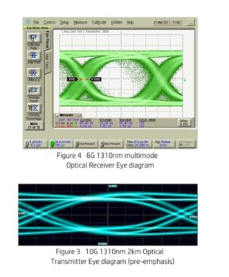
We know that the eye diagram is the digital signal (the general NRZ code) of the many unit serial graphics superposition, because the graphics similar to the eye, it is called eye diagram. It fully characterizes the bit information of the serial signal, and becomes a simple and important tool to measure the signal quality, and is the most direct and effective method for the transmission performance observation of binary digital signals. In order to facilitate the rapid evaluation of eye diagram quality, the different rates, the different photoelectric performance of the optical transceiver module, the relevant standards set a measure of the eye map qualified or not “eye pattern.” Generally, the optical eye and the electrical eye of the optical transceiver module with a transmission rate of less than 2.5Gb/s are easy to meet the requirement of the eye pattern. The eye line is usually a single line. However, the optical transceiver module with a transmission rate of 2.5Gb/s or more, Its eye diagram lines often appear double or multi-line. Figure 1, 2 are 10Gb/s 1310nm multi-mode optical transceiver module at 25 ℃ and 85 ℃ test results. Figure 2 Eye edge “hairiness” and eye pattern edge margin is poor than Figure 1. Figure 3 is a pre-emphasis 10Gb/s optical transceiver light eye diagram, the figure clearly shows the upper and lower left and right eyeliner has two. Figure 4 for the 6G, multi-mode, 1310nm optical receiver module electric eye diagram. In the figure, the rising edge of the eye is a thick, double hairline, and the descending edge appears to have a noticeable noise.
APD low-temperature light saturation problem
For high-speed optical transceiver modules for engineering applications, we typically perform high and low-temperature cycling and storage tests at -40 ° C and 85 ° C. It was found that some products of 2.5Gb/s high sensitivity light receiving module with APD-TIA ROSA had low saturation optical power. That is, after storage at -40 ℃, part of the light receiving module saturation (or overload) optical power is low, lower than the relevant standard 8dBm optical power requirements, the test results shown in Table 1. In order to facilitate comparison, also listed at 25 ℃, 85 ℃ other optical receiver module sensitivity saturation optical power normal test results.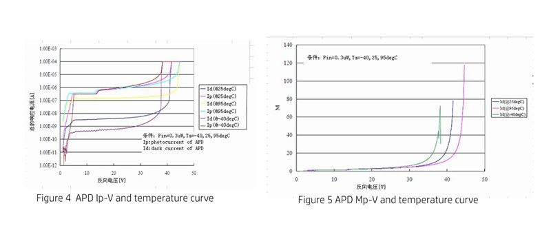 Table 1 shows that the light receiving sensitivity and saturation optical power of the 2.5Gb/s optical receiver module with APD-TIA ROSA meet the specified requirements at 25 ° C and 85 ° C ambient temperature, but some of the light receiving modules are at -40 ° C Under the saturation of optical power is less than -8dBm, does not meet the product saturation optical power requirements of indicators. This result seems to make people feel abnormal. It is generally believed that semiconductor photodetectors and microelectronic integrated circuits are temperature-sensitive devices, the lower the temperature, the photoelectric properties should Be better.
Hello,nice share.